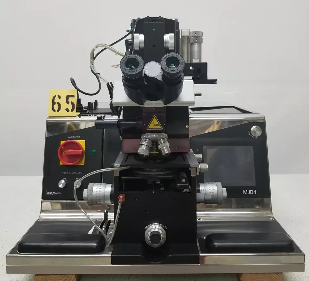
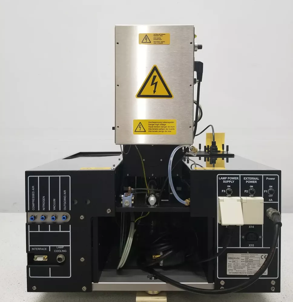
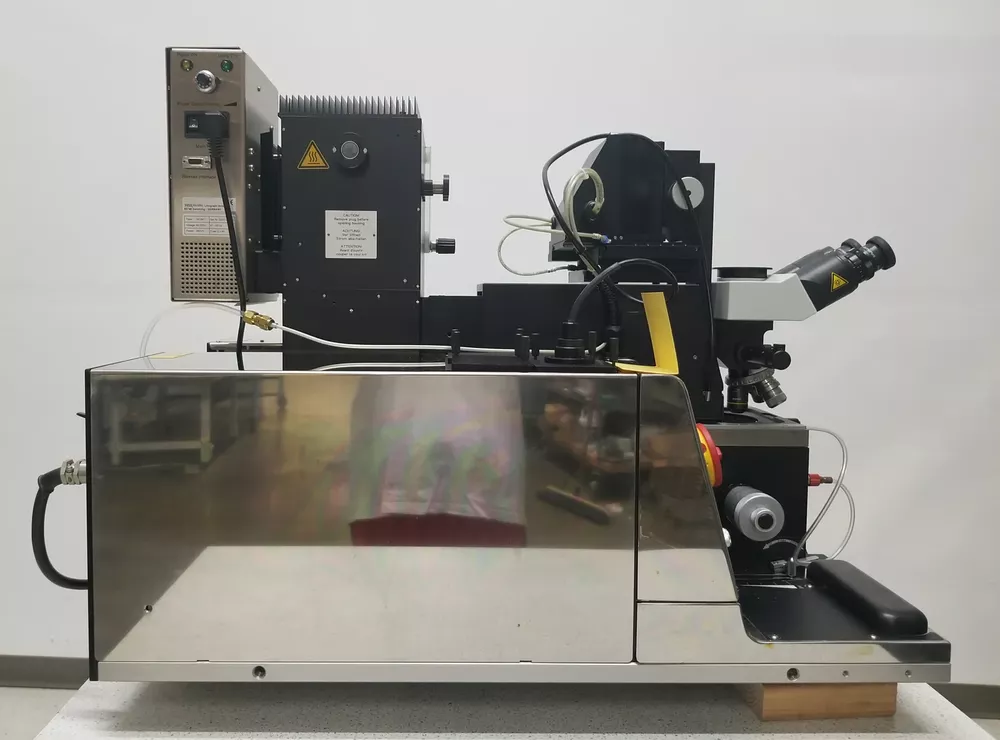
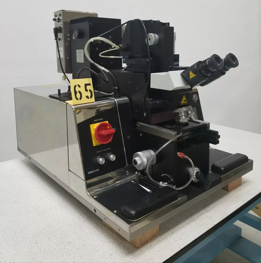
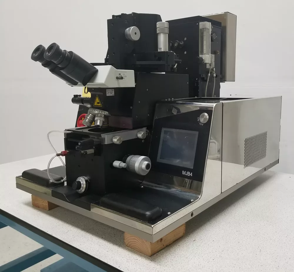
Suss MicroTec MJB4
AMERICA North (USA-Canada-Mexico)
• System Type: Mask aligner and UV exposure system
• Application: Laboratory use
• Application: Small series production
• Exposure Mode: Contact exposure
• Resolution: 0.5 µm
• Application Field: MEMS
• Application Field: Optoelectronics
• Substrate Type: Hybrids
• Substrate Type: High frequency components
• Substrate Type: GaAs
• Substrate Type: InP
• Microscope Type: SUSS split field microscope
• Alignment Stage Type: XY Theta stage
• X Travel Range: ±5 mm
• Y Travel Range: ±5 mm
• Theta Travel Range: ±5°
• Spindle Type: High precision backlash-free micrometer spindles
• Substrate Thickness Compensation: Adjustable
• Z Movement: Manual
• Maximum Substrate Thickness: 4 mm
• Maximum Wafer Diameter: 100 mm
• Maximum Substrate Size: 4 in x 4 in
• User Interface: Touch panel graphical interface
• Operation: Ergonomic design